so, let's start, the first issue I have with ampere is the manufacturing node, yes, even that tells us some things, the ampere cards are Samsung 8nm.
because it tells us some things about the NVIDIA plan with ampere.
sure, it means that NVIDIA was offered a price too high by TSMC for manufacturing the ampere cards and that means they did know that there was a shortage coming all along.
I wish, I really do.
so, let's start from the beginning, the die and substrate. the 3090 has a 628 mm² die and it has a 350W TDP (it peaks at 600-650W but we will go back to this later)
it's actually surprisingly simple to understand, the die itself if silicon, it's massive and pulls a ton of power which becomes mostly heat.
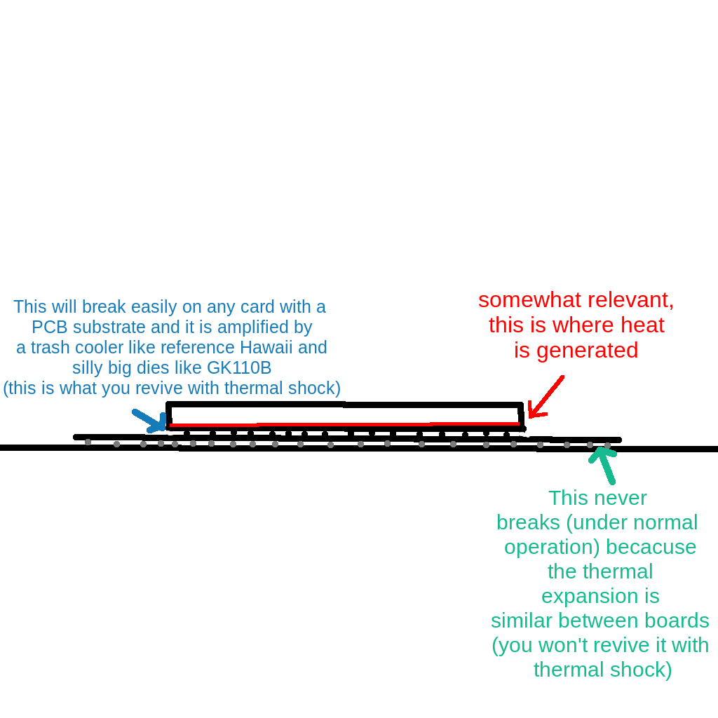
well, the most common failure for NVIDIA cards, especially historically (pretty much anything I remember other than Pascal and low end Maxwell is afflicted by this) and it is the concept of thermal cycling. a GPU die is connected to a substrate (the green interconnect PCB which is soldered to the PCB of the card) using and that connection is bound to break with thermal expansion because silicon and the PCB (copper and fiber glass) have extremely different thermal expansion behaivour. This is amplified by the die being larger because a larger die means that the silicon will expand more and to make matters worse a larger die is also more power hungry and runs hotter making the temperature delta between idle and full load bigger.
not even close, sadly.
well, the next one is the VRM or power delivery, NVIDIA started selling FE cards but those are not to be confused with the reference design, which is often worse. Which is very apparent with 3090s, the reference design (seen on cheaper cards like the Gigabyte 3090 Eagle and Vision is very poor and not good enough for the Ampere peaks, while yes it does handle the 350W sustained it doesn't handle the peaks in the slightest and the power monitoring NVIDIA adopted is... an average measurament! yes, really... despite the voltage controller clearly supporting in-rush monitoring, NVIDIA decided to disable it and take their usual shunt resistor approach! this is not fine because the shunt resistor approach is slower and not nearly as accurate but it allows for questionable usefullness power balancing on multi rail power supplies and most importantly was already implemented in the driver!
remember the new world killing 3090s disaster? well, it happened because of this. no, new world was not written poorly, if anything, it was written efficently causing huge power spikes, causing extreme transients on the VRM which turns in a lot of strain for the mosfets which ultimately end up breaking, the weakest mosfet in a VRM is obviously the low side which means your GPU core is getting a journey at 12V (depending on how quickly OCP trips on the PSU you might go destroy the die to the point where it doesn't even attempt to boot or you might get lucky and fixing the VRM is enough to make the card work again).
sadly, yes, there's more, and arguably the most discussed out of these issues.
yeah, the cards don't properly cool the GDDR6X chips which might cause thermal cycling on those too! (they use an insane amount of power if you didn't know) as if that wasn't enough, they don't really have any benefit on NVIDIA cards because the NVIDIA GPUs have other bottlenecks before VRAM becomes the issue, which is rather odd but I won't question it. I guess, if you care about morality, GDDR6X was such a fair move against AMD that NVIDIA has the exclusive on it, even if AMD cards are the ones that truly benefit from faster VRAM, I am not going to use this as a point as it is highly subjective, same goes for the NVIDIA drivers not being good.
(I will do other rants like this in the future about other hardware, I have a lot in mind but it takes time and effort to get a shareable opinion on things).
here's your navigation buttons, as much as I find them silly.
Blog Index Main Page