I must first of all mention that this wasn't easy, I've tried for years before even getting to my first success, before it I could clean up boards after pulling big chips, I could do small chips chips just fine but I had never gotten as far as a ram chip.
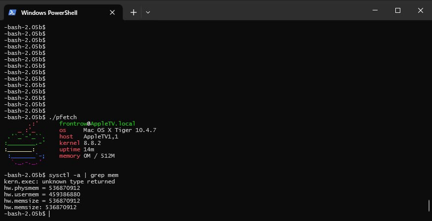
after some inspiration one night I decided to give bga work another shot after recently getting really close on some scrap board and took a random small ddr2 dimm and figured it would be a good candidate because of the small mass and near zero value in case it didn't end up working out. and here's how that went:
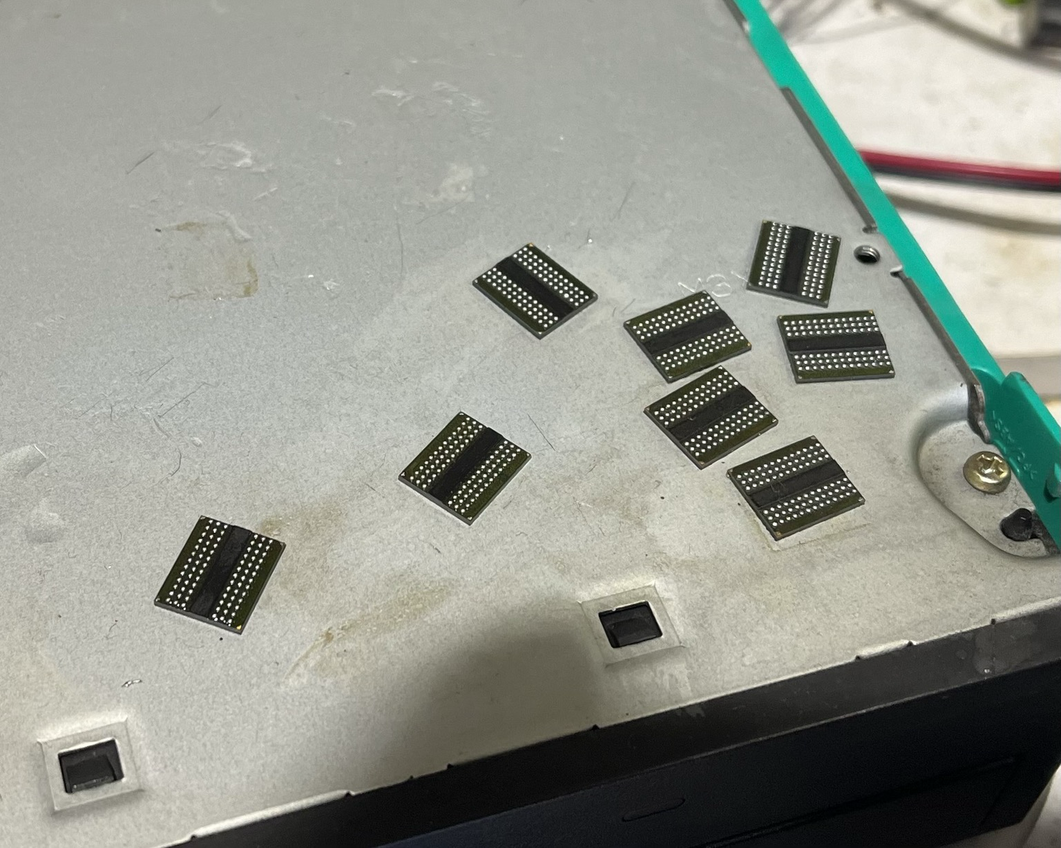
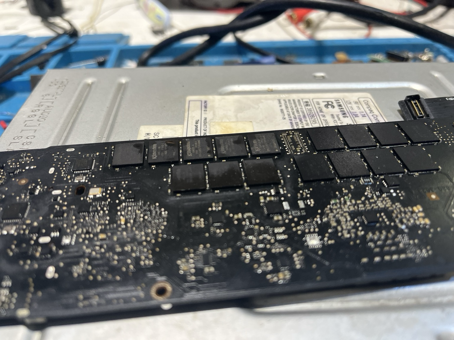
Now that I got the hang of it I started getting confident in my skills and this is when I took an i7 MacBook Air 4,2 board and a Dual Rank 8GB DDR3L SODIMM and decided to transplant the 4Gbit ICs over to the MacBook board. At the time I didn't consider just how long manually reballing 16 ICs (1536 balls) without stencils would take but you know what? The board was sketchy to begin with so I figured there was nothing to lose. I also expected to be able to only switch over one bank at a time and use coreboot to debug but I ended up being forced to swap around both banks before I could get any real training success.
I must admit having coreboot logs and a decent way to inject SPD makes debugging much easier, I ended up dumping the stock SPD from the SODIMM, patching it to be single rank and fixing the checksums (good thing I did because these chips turned out to be a less common row column setup that is incompatible with the stock spd).


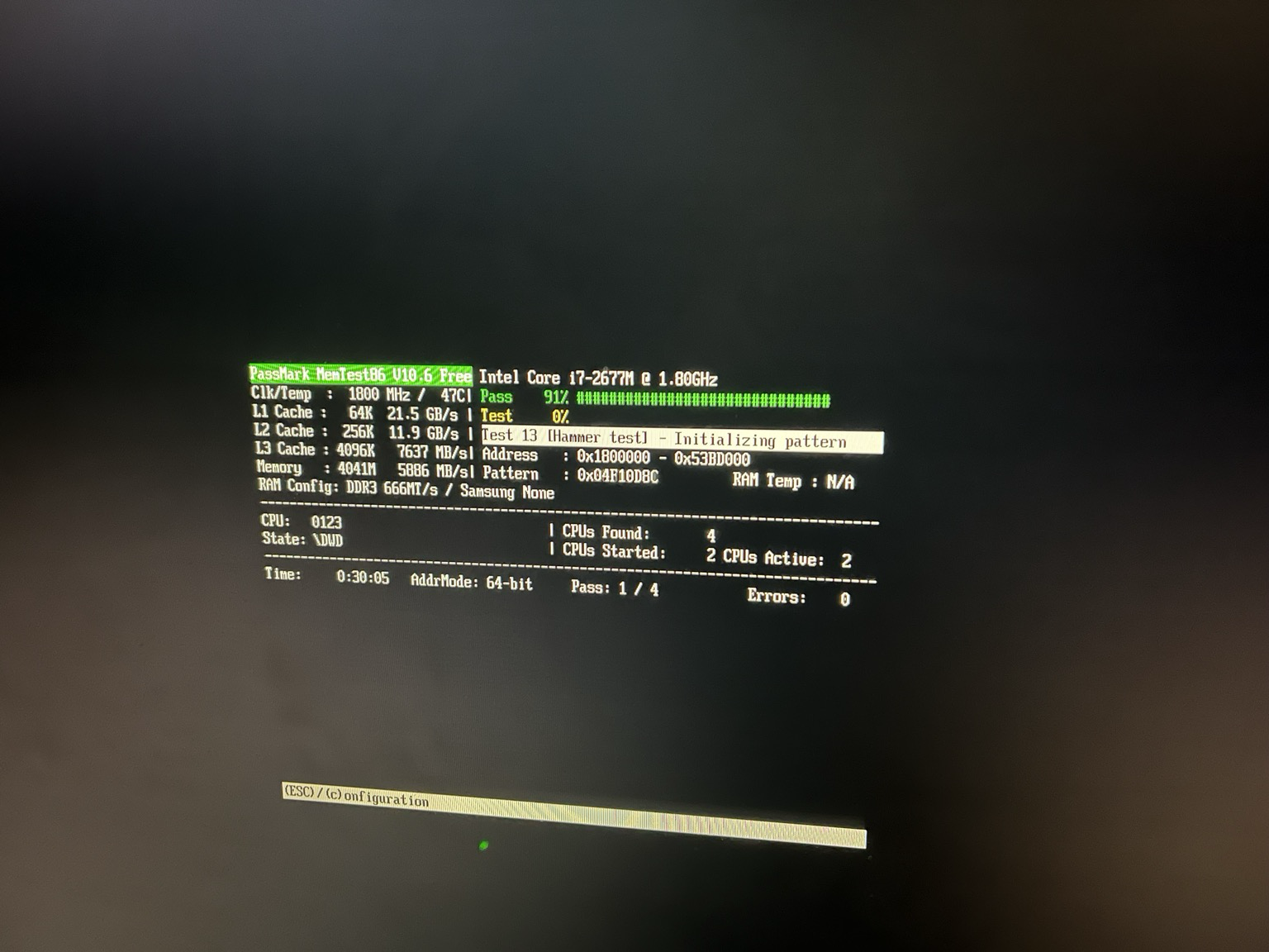
Unfortunately problems weren't over, when I got to boot seabios I realised my board would reboot the second memtest86+ addressed over 4GB of memory and it seemed very odd to me considering the framebuffer didn't have any obvious artifacting. this was further confirmed by booting linux limiting the maximum addressable ramspace using the mem=4G flag, at first I figured one I had some kind of bridge or ram failure but I quickly realised that Apple simply never routed the extra address line required to address the the upper half of memory, I thought apple shipped these boards in 8GB configurations but unfortunately I was confusing this board for the 5,2 2012 variant that routes the extra lanes.

Making the board usable was pretty straight forward, I had to patch byte 0x4 and 0x5 on the SPD which tells the memory controller to treat the chip as a 2Gbit one and this worked flawlessly on coreboot but didn't instantly work on the OEM firmware, eventually when I came back to it with a fresh mind I realised I was patching the EFI module wrong which broke the EFI integrity signatures.
Now that I'd gotten confident at this kinda work I decided that it would be time to do something completely pointless and obsolete just because when I originally stubmled upon this I couldn't do it.
Honestly there's not too much to say on this one, the software side was very similar to the MacBook Air 4,2 OEM firmware patches. The hardware side was easier than the previous project because it was only 4 ICs and in DDR2 footprint (which is easier to reball). The only interesting thing here is that apparently some ddr2 sodimms are Dual Rank x16 instead of Single Rank x8 which would be the same pin count and "more standard". Good for us because this means it's easier to source the ICs needed for this upgrade on 1GB SODIMMs

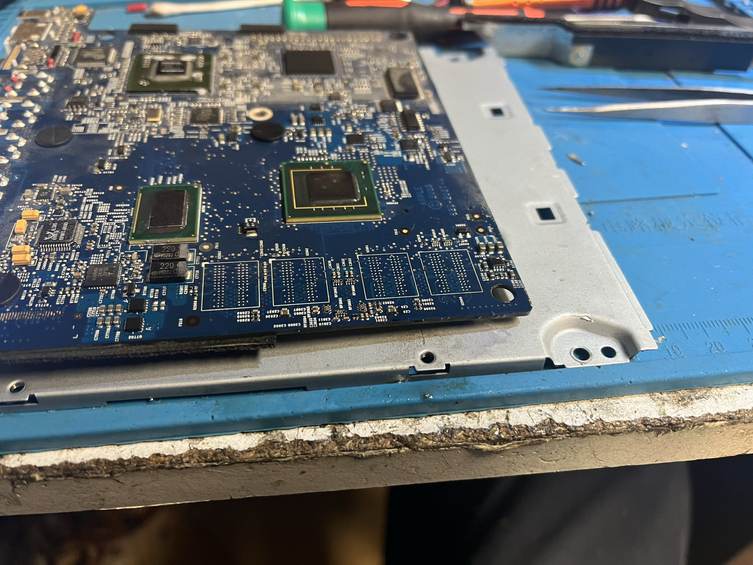

Now, after having gotten more familiar with BGA work it was time for a big project, something that is actually economically viable... but also something that is far riskier... This is when I got lucky, a friend of mine (thank you again!) shipped me a Steam Deck at this point my objective was simple... Upgrade the RAM!.
I knew this would be doable to from the jump because I had seen people do it before and I even found the a python script to patch "APCB" modules that contain SPD data but also just patched up bioses in flashable format.
Now, my first task was figuring out what chips to solder on it. I wanted parts that I could clock up from stock but I also didn't want to spend an arm and a leg on the chips. This is why I chose to go for samsung parts, hynix parts would've probably been faster but they were also significantly more expensive and untested.
Unfortunately like most projects there's always gonna be some complications and in this case it was the aliexpress seller sending my 16GB parts, it took me a good hour of debugging to figure out that yes indeed I did the work properly but unfortunately with the wrong part.
Here is the video of how it went:
Fortunately after figuring out what went wrong I decided to keep going and ordered some more this time making sure I was getting the right density.
Well, now that I verified that I know what I am doing I'll finally be able to get my upgrade done, right?
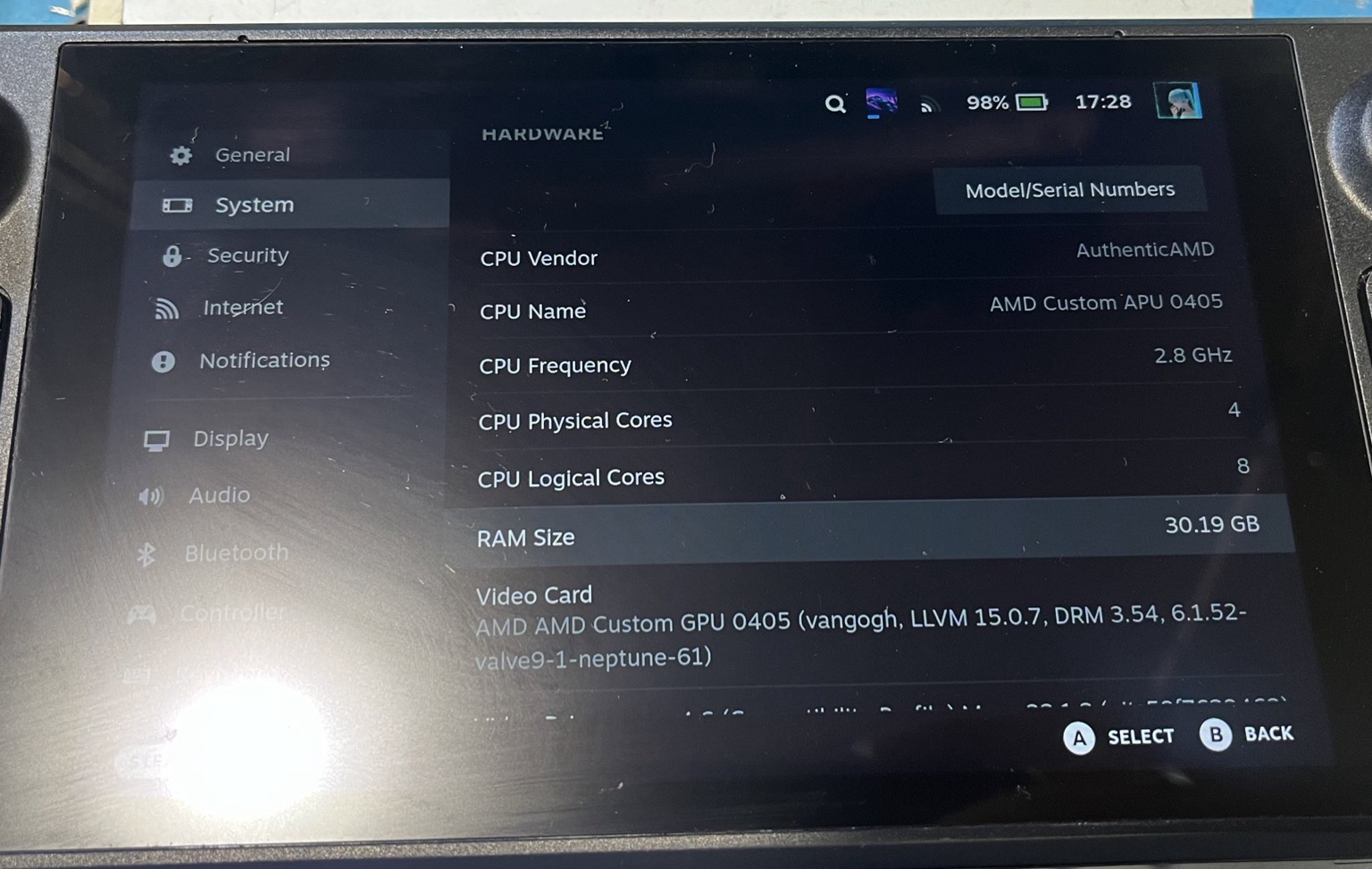
As it turns out, not really, in soldering the chips one of them bridged and I had to spend an hour reballing it before I could finally get it to boot again, I flashed the 32GB bios and what do you know? I finally get this forbidden sight:
Here's the video for the second, successful attempt:
here's your navigation buttons, as much as I find them silly.
Blog Index Main Page